
 +++lead-in-textnnIn August, chipmaker [Intel](https://www.wired.com/tag/intel/) revealed new details about its plan to build a “mega-fab” on US soil, a $100 billion factory where 10,000 workers will make a new generation of powerful processors studded with billions of transistors.The same month, 22-year-old Sam Zeloof announced his own [semiconductor](https://www.wired.com/tag/intel/) milestone.It was achieved alone in his family’s New Jersey garage, about 30 miles from where the first transistor was made at Bell Labs in 1947.nn+++nnWith a collection of salvaged and homemade equipment, Zeloof produced a chip with 1,200 transistors.He had sliced up wafers of silicon, patterned them with microscopic designs using ultraviolet light, and dunked them in acid by hand, documenting the process [on YouTube](https://www.youtube.com/watch?v=IS5ycm7VfXg) and [his blog](http://sam.zeloof.xyz/second-ic/).
“Maybe it’s overconfidence, but I have a mentality that another human figured it out, so I can too, even if maybe it takes me longer,” he says.nnZeloof’s chip was his second.He made the first, much smaller one as a high school senior in 2018; he started making individual transistors a year before that.His chips lag Intel’s by technological eons, but Zeloof argues only half-jokingly that he’s making faster progress than the semiconductor industry did in its early days.
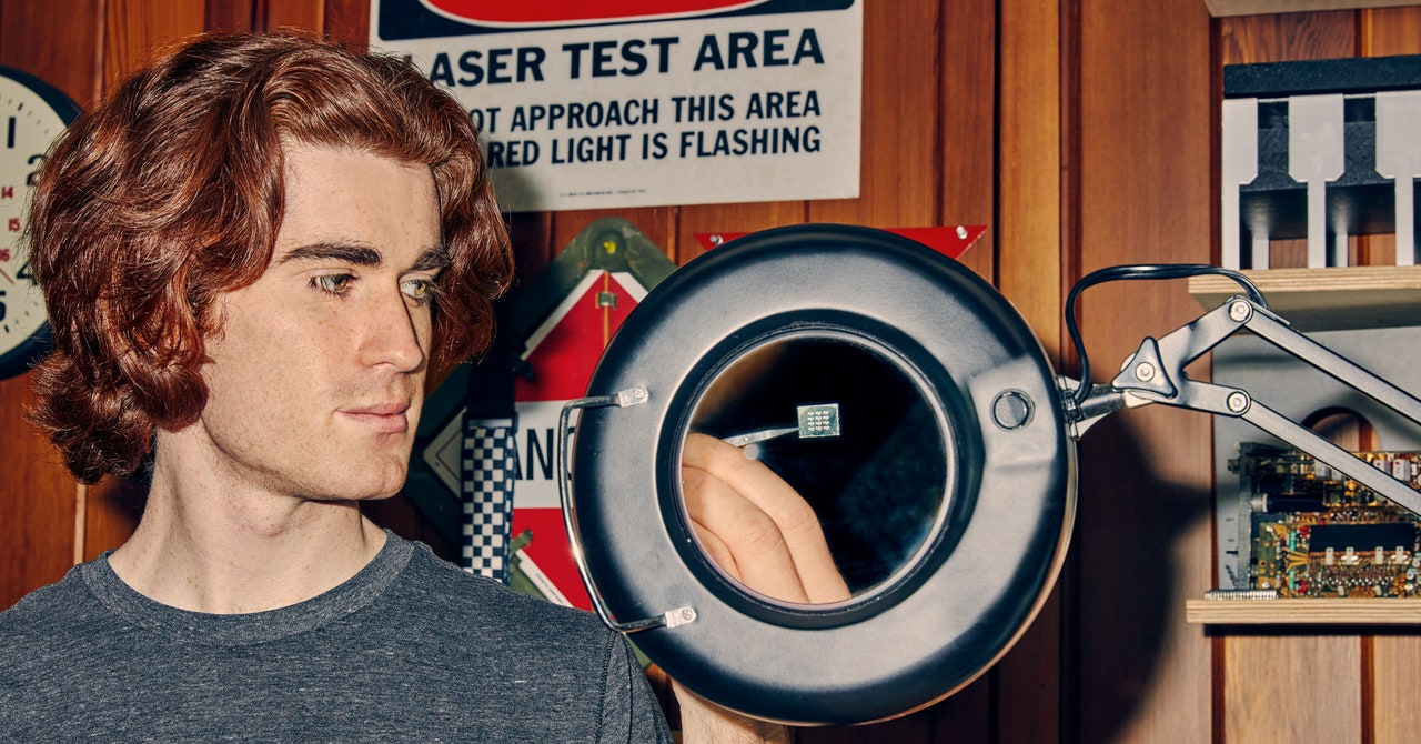
His second chip has 200 times as many transistors as his first, a growth rate outpacing Moore’s law, the rule of thumb coined by an Intel cofounder that says the number of transistors on a chip doubles roughly every two years.nnZeloof now hopes to match the scale of Intel’s breakthrough 4004 chip from 1971, the first commercial microprocessor, which had 2,300 transistors and was used in calculators and other business machines.In December, he started work on an [interim circuit design](https://twitter.com/szeloof/status/1479847749822685184) that can perform simple addition.nnnn[#image: /photos/61e7533702a1a063b0506075]|||Zeloof says making it easier to tinker with semiconductors would foster new ideas in tech.|||nnOutside Zeloof’s garage, the pandemic has triggered a global semiconductor shortage, hobbling supplies of products from [cars](https://www.wired.com/story/silicon-chip-shortage-automakers/) to [game consoles](https://www.wired.com/story/gaming-console-sellers/).That’s inspired new interest from policymakers in [rebuilding the US capacity](https://www.wired.com/story/us-needs-back-business-making-chips/) to produce its own computer chips, after decades of offshoring.nnGarage-built chips aren’t about to power your PlayStation, but Zeloof says his unusual hobby has convinced him that society would benefit from chipmaking being more accessible to inventors without multimillion-dollar budgets.
“That really high barrier to entry will make you super risk-averse, and that’s bad for innovation,” Zeloof says.nnZeloof started down the path to making his own chips as a high school junior, in 2016.He was impressed by YouTube videos from inventor and entrepreneur Jeri Ellsworth in which she [made her own, thumb-sized transistors](https://www.youtube.com/playlist?list=PL5DCEA197C1C07A2D), in a process that included templates cut from vinyl decals and a bottle of rust stain remover.Zeloof set out to replicate Ellsworth’s project and take what to him seemed a logical next step: going from lone transistors to integrated circuits, a jump that historically took about a decade.“He took it a quantum leap further,” says Ellsworth, now CEO of an augmented-reality startup called [Tilt Five](http://www.tiltfive.com).
“There’s tremendous value in reminding the world that these industries that seem so far out of reach started somewhere more modest, and you can do that yourself.”nnComputer chip fabrication is sometimes described as the world’s most difficult and precise manufacturing process.When Zeloof started blogging about his goals for the project, some industry experts emailed to tell him it was impossible.
“The reason for doing it was honestly because I thought it would be funny,” he says.“I wanted to make a statement that we should be more careful when we hear that something’s impossible.”nnZeloof’s family was supportive but also cautious.His father asked a semiconductor engineer he knew to offer some safety advice.“My first reaction was that you couldn’t do it.This is a garage,” says Mark Rothman, who has spent 40 years in chip engineering and now works at a company making technology for OLED screens.
Rothman’s initial reaction softened as he saw Zeloof’s progress.“He has done things I would never have thought people could do.”nnZeloof’s project involves history as well as engineering.Modern chip fabrication takes place in facilities whose expensive HVAC systems remove every trace of dust that might trouble their [billions of dollars of machinery](https://www.wired.com/story/asml-extreme-ultraviolet-lithography-chips-moores-law/).
Zeloof couldn’t match those techniques, so he read patents and textbooks from the 1960s and ’70s, when engineers at pioneering companies like Fairchild Semiconductor made chips at ordinary workbenches.“They describe methods using [X-Acto](https://www.wired.com/story/how-x-acto-knife-went-from-battlefields-to-craft-rooms/) blades and tape and a few beakers, not ‘We have this $10 million machine the size of a room,’” Zeloof says.nnZeloof had to stock his lab with vintage equipment too.On eBay and other auction sites he found a ready supply of bargain chip gear from the 1970s and ’80s that once belonged to since-shuttered Californian tech companies.Much of the equipment required fixing, but old machines are easier to tinker with than modern lab machinery.One of Zeloof’s best finds was a broken electron microscope that cost $250,000 in the early ’90s; he bought it for $1,000 and repaired it.He uses it to inspect his chips for flaws, as well as the [nanostructures on butterfly wings](https://www.youtube.com/watch?v=OSkeIcz9SqI).nnnn[#image: /photos/61e75338a098d1434bc8584d]|||Zeloof fixes up obsolete equipment bought online, including an electron microscope, to make his chips.|||nnAt times Zeloof had to improvise.
As in a real chip fab, he wanted to transfer his microscopically detailed designs onto his devices using a process called photolithography.It involves coating a chip-to-be in light-sensitive material and using a device like a super-precise projector to burn in a template that will guide subsequent processing steps.
Photolithography machines are expensive—[up to $150 million](https://www.wired.com/story/asml-extreme-ultraviolet-lithography-chips-moores-law/)—and so Zeloof made his own by bolting a modified conference room projector bought on Amazon onto a microscope.It projects his designs at tiny scale onto silicon wafers that Zeloof coats in material sensitive to ultraviolet light.nnIn 2018, Zeloof designed his first chip, a simple amplifier with six transistors, during gym class after a substitute teacher directed students to do class work.After about 12 hours of work and 66 steps in his garage, he had the Z1.It featured three of the dancing bears that are a symbol of the Grateful Dead and now appear on all of Zeloof’s chips, in a nod of thanks to Rothman, a fan of the band.nnThe Z1 used transistors that Zeloof calls “straight out of the 1970s,” with features as small as 175 microns, roughly a hairsbreadth.He put the chips to work in a circuit board that flashes a single LED and a [guitar distortion pedal](https://twitter.com/szeloof/status/1280249239495479297).nnLate in 2018, Zeloof started at Carnegie Mellon University, hacking on pieces of garage fab equipment in his dorm room while studying electrical engineering.Although he says he followed safety protocols, the university took exception to the x-ray machine in his dorm room.During trips home, he upgraded his setup in preparation for his second chip, the Z2.It uses a faster-switching transistor design based on wafers of a form of crystalline silicon known as polysilicon that became dominant in the 1970s.nnZeloof spun hand-cut, half-inch squares of polysilicon, each to become a separate chip, on a small homemade turntable at 4,000 revolutions per minute to coat them with the photosensitive material needed to transfer his design onto the surface.
Then his homemade photolithography machine beamed on his design: a grid of 12 circuits, each with 100 transistors (and a dancing bear), 1,200 transistors in all.nn+++feature-largenn+++group-3nn[#image: /photos/61e75336e365ac4c375307f8]|||Zeloof’s first chip, the Z1, was made in 2018 when he was still in high school and has six transistors.|||nnnn[#image: /photos/61e7533b418ddba38e293c8e]|||His second chip, the Z2, was finished in August 2021 and has 1,200 transistors.|||nnnn[#image: /photos/61e75335e365ac4c375307f6]|||Zeloof is working on the Z3, a chip that will be capable of adding 1 \+ 1, as a step to a full microprocessor.|||nn+++nn+++nnEach chip was then etched with acid and cooked in a furnace at about 1,000 degrees Celsius to bake in phosphorus atoms to adjust its conductivity.Three more rounds under the photolithography machine—separated by steps including time in a vacuum chamber filled with glowing purple plasma to etch away polysilicon—finished off each chip.Today’s commercial fabs produce chips in a broadly similar way, using a sequence of steps to gradually add and remove material in different parts of a design.Those chips are much more complex, with billions of much smaller transistors arrayed tightly together, and the steps are performed by machines not by hand.The transistors on Zeloof’s second-generation chips were about 10 times faster than those on his first and had features as small as 10 microns, not much bigger than a red blood cell.nnIn August, Zeloof tested the Z2 by hooking it up to a boxy beige semiconductor analyzer released by Hewlett Packard about two decades before he was born.
A series of smoothly ramping current-voltage curves on its glowing green screen signaled success.“That curve was amazing to look at,” Zeloof says, “the first sign of life after you spend all day dunking this little shard of crystals into beakers of chemicals.”nnHow to celebrate when your homemade chip works? “[Tweet it\!](https://twitter.com/szeloof/status/1426320030292189186)” Zeloof says.His project has earned a dedicated Twitter following and millions of YouTube views, as well as some handy tips from veterans of the 1970s semiconductor industry.nnZeloof says he doesn’t know for sure what he wants to do after graduating this spring, but he has been thinking about the place DIY chipmaking might have in the modern tech ecosystem.In many ways DIY experimentation has never been more powerful: Robotics gear and 3D printers are easily bought, and hacker-friendly hardware like the Arduino microcontroller and [Raspberry Pi](https://www.wired.com/tag/raspberry-pi/) are well established.
“But the chips are still made in a big factory somewhere,” Zeloof says.“There’s been little progress with making that more accessible.”nnEllsworth, whose homebrew transistors inspired Zeloof, says there could be value in enabling high-quality hands-on chipmaking.“The tools we have today could put this within reach of small-scale operations, and for certain problems I think it makes a lot of sense,” she says.Ellsworth says chip technology seen as outdated to leading fabs can still be useful to engineers.nnZeloof recently upgraded his photolithography machine to print details as small as about 0.3 microns, or 300 nanometers—roughly on par with the commercial chip industry in the mid-’90s.Now, he’s thinking about the functions he could build into a chip on the scale of Intel’s historic 4004.
“I want to push garage silicon further and open people’s minds to the possibility that we can do some of this stuff at home,” he says.nn***n### More Great WIRED Storiesn- 📩 The latest on tech, science, and more: [Get our newsletters](https://www.wired.com/newsletter?sourceCode=BottomStories)\!n- The race to [find “green” helium](https://www.wired.com/story/green-helium-mining/?itm_campaign=BottomRelatedStories&itm_content=footer-recirc)n- [Covid will become endemic](https://www.wired.com/story/covid-will-become-endemic-the-world-must-decide-what-that-means/?itm_campaign=BottomRelatedStories&itm_content=footer-recirc).What happens now?n- A year in, [Biden’s China policy](https://www.wired.com/story/biden-china-policy-looks-like-trumps/?itm_campaign=BottomRelatedStories&itm_content=footer-recirc) looks a lot like Trump’sn- [The 18 TV shows](https://www.wired.com/story/most-anticipated-tv-2022/?itm_campaign=BottomRelatedStories&itm_content=footer-recirc) we’re looking forward to in 202n- How to guard against [smishing attacks](https://www.wired.com/story/smishing-sms-phishing-attack-phone/?itm_campaign=BottomRelatedStories&itm_content=footer-recirc)n- 👁️ Explore AI like never before with [our new database](https://www.wired.com/category/artificial-intelligence/?itm_campaign=BottomRelatedStories&itm_content=footer-recirc)n- 📱 Torn between the latest phones? Never fear—check out our [iPhone buying guide](https://wired.com/gallery/iphone-buying-guide/?itm_campaign=BottomRelatedStories&itm_content=footer-recirc) and [favorite Android phones](https://wired.com/gallery/best-android-phones/?itm_campaign=BottomRelatedStories&itm_content=footer-recirc)nn.